|
In part one we covered the two hardware address spaces in the PIC® MCU and how they can be used from C. Part two explained how a developer defines virtual address spaces. In this article we will detail how some PIC® MCUs have their own alternative address spaces and how the C compiler deals with them.
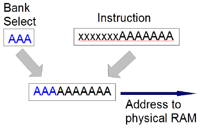
First, we must have a basic understanding about the fundamental addressing at the hardware level. Consider a PIC16F887 part and the instruction to add a memory value to the working register and put the result in the working register. The 14 bit instruction looks like this:
0 0 0 1 1 1 0 a a a a a a a
The aaaaaaa is the address in memory to get the data from. Notice there are only 7 bits so the address range is 0-127. In order to gain access to the rest of memory, there are some bank select bits. If the bank select bits are set to 010 then the instruction with aaaaaaa set to 0000001 will actually access memory location 0100000001. Fortunately, the compiler (at least the CCS C compiler) takes care of setting the right bank select bits before any instruction that needs the bits changed. There is a similar method used for program memory where the bits are called the page select bits. That comes into play with goto's and calls.
The following topics cover special features in some PIC® MCU parts that allow for a more effective way to access memory.
Mid-range Shared RAM
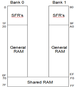
Even the old PIC chips had some special function registers duplicated in every bank, so there is no need to switch banks to access a popular register, like the status register. Many of the newer PIC® MCUs also have some general purpose RAM duplicated in all the banks. For example, on the PIC16F887 locations 0x70-0x7F reference the same RAM locations regardless of the bank bit setting. That means 0x70 and 0x1F0 are the same location. It is for this reason the compiler scratch locations begin at 0x70.
Mid-range Linear Address Space
On the mid-range parts the special function registers typically are at the start of each bank. For example 0x00 to 0x1F are SFR and 0x20-0x7F is general RAM. Then 0x80 to 0x1F are SFR and 0xA0 to 0xFF has general RAM. This means the largest data structure a user can have in RAM is 96 bytes or 80 bytes if there is shared RAM. If the user needs a larger array for example, they would need to split it into two smaller arrays.
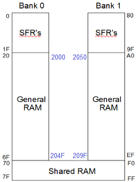
On some mid-range PIC® MCUs there is an extended instruction set (4 and 5 digit parts after the F). In these parts there is a second way to access RAM called linear addressing. The linear address space has all the general purpose RAM locations and none of the SFR's. The entire general purpose RAM is put at location 0x2000 and up. Location 0x2000 is the same as 0x20. Location 0x02050 is the same as 0xA0. Now users can have data structures as large as memory can hold. The only way to address using the linear method is using indirection via the FSR registers. In the CCS C Compiler anytime a user accesses a data item using a variable index the linear addressing method is used if available on the part.
PIC18 Access Space
On the PIC18 parts most instructions have what is called an access bit to select what address space is used in the instruction. In the normal mode, the addressing works like the PIC16 using bank select bits somewhere else to fully specify the address. However, if the access bit is 0 then the address in the instruction is used to access only certain registers. The add instruction on the PIC18F4520 looks like this:
0 0 1 0 0 1 0 x a a a a a a a a
When x (the access bit) is 1 the address in the instruction is combined with the bank select bits to form the physical address.
When x is 0 then the physical address depends on the value of the address. With lower addresses then the remaining address bits are used as-is to get the physical address without using the bank select bits. For example, 00000001 will give users physical address 1 regardless of the bank select bit setting. This is kind of like the shared RAM feature in the PIC16. When the address is higher (0x80 and up on the PIC18F4520) then 0xF80 is added to the address over the cutoff to get the physical address. This allows for access to special function registers regardless of the bank select bit setting. Be aware however that different PIC18 parts have a different split between general purpose RAM and the SFR's in the access space. The PIC18F4520 has 128 bytes in each however the PIC18F4550 has only 96 bytes in general RAM and the rest in SFR's.
It should also be pointed out the PIC18 has a special double word instruction that can copy from any RAM address to any other RAM address.
PIC18 XINST
Most PIC18 parts have a XINST bit in the configuration fuses. When this bit is set the way the general purpose RAM is accessed when the access bit is set is modified. Instead of accessing the RAM directly the address is first added to the contents of another register. The intent with this feature is to make the using local variables easier in C code where users could have variables on a stack. This would allow for recursive functions. Since this feature is either on or off for the whole CCS has decided not to add support in the compiler for XINST because of the rare need for recursion and the inefficiencies caused by using this mode.
PIC24/DSPIC Extended RAM
On the 24 bit parts, the bank select bits were removed. Looking at the same add instruction it looks like this:
1 0 1 1 0 1 0 0 0 0 0 a a a a a a a a a a a a a
That means the instruction has direct access to RAM locations 0-1FFF (8K). That is a lot but many of these parts have more RAM than that. There are two ways to access RAM above 1FFF. First is to indirectly access the RAM using a 16 bit pointer (64K). This does require an extra instruction or two but is not as bad as it sounds since many instructions allow indirect addressing using one of the working registers. The other method is to use a special instruction to copy to/from any address 0-FFFF (64K) and a working register.
In summary, we have a great way to access 8K of RAM and there is a method to get at RAM over 8K but the method needs to be repeated for each access.
PIC24/DSPIC PSV Mode
Access to program memory (for constants) requires some extra steps to set up some registers and grab the data. The 24 bit parts have a mode that can be used to map the upper 32K of RAM addresses on to a selected area of program memory. This can be used to access constants in program memory as easily as if they were in RAM. When doing this, users loose access to the upper 32K of RAM. By default the CCS Compiler does not use this technique because in general it seems additional RAM is more important than fast access to ROM. A lot of the Microchip example code does use PSV mode so there is support in the CCS compiler to allow for easier porting.
#device PSV=16 // Turns on PSV mode
const char serial_number[] = {"123456789"}; // Saved in ROM
...
sn = atol32(serial_number); // Is accessed by a RAM address
Like us on Facebook. Follow us on Twitter.
About CCS:
CCS is a leading worldwide supplier of embedded software development tools that enable companies to develop premium products based on Microchip PIC® MCU and dsPIC® DSC devices. Complete proven tool chains from CCS include a code optimizing C compiler, application specific hardware platforms and software development kits. CCS' products accelerate development of energy saving industrial automation, wireless and wired communication, automotive, medical device and consumer product applications. Established in 1992, CCS is a Microchip Premier 3rd Party Partner. For more information, please visit https://www.ccsinfo.com.
PIC® MCU, MPLAB® IDE, MPLAB® ICD2, MPLAB® ICD3 and dsPIC® are registered trademarks of Microchip Technology Inc. in the U.S. and other countries.
|


