 |
 |
| View previous topic :: View next topic |
| Author |
Message |
temtronic
Joined: 01 Jul 2010
Posts: 9115
Location: Greensville,Ontario


|
|
 Posted: Thu Mar 23, 2017 5:55 am Posted: Thu Mar 23, 2017 5:55 am |
 |
|
I have to back RF-D 100% about 'do not use simulators' ! NONE can 'simulate' te Real World, none, it ain't going to happen. Like WHO would inject data on one pair of a 50 pair cable that your data is also using one pair ,just to see if crosstalk 'degrades' your data? No one. The Real World did though !
I've followed this topic for several reasons. One, there is an easy way to achieve the original requirement of a '1V rectified sine wave' but the OP insists on misusing technology in an attempt to achieve the goal. As stated several times the chosen PIC doesn't have active I2C terminators,so is the wrong choice,unless additonal components are used. I see the 'higher speeds' I2C same as 'overclocking', trying to get more for less.Same as getting 300HP from a 4cyl. engine that originally was 25HP. Abusing the wrong tools for the job is never a good idea.
Jay |
|
 |
viki2000
Joined: 08 May 2013
Posts: 233
|
|
|
temtronic
Joined: 01 Jul 2010
Posts: 9115
Location: Greensville,Ontario
|
|
| Posted: Thu Mar 23, 2017 7:26 am |
|
|
I can't say which is 'best'. Once you get parts and bench test , you'll soon see a lot of the 'theory' ain't worth the paper it's printed on! After 40+ years in the analog world and the only true way to confirm 'stuff works' is to bench test. It's all in the details that no onethinks about, type of PCB, trace thicknesses,width, wrong caps,cell phones,etc...I recall a PhD dude swear according to the math, 'it won't work' , but 15 minutes on the bench, I showed him it did..and better than 'the math'.
Jay |
|
|
newguy
Joined: 24 Jun 2004
Posts: 1902
|
|
| Posted: Thu Mar 23, 2017 7:53 am |
|
|
There's something you've been missing and quite a few people have been trying to inform you about it. I'm going to take a different approach. Here's your assignment:
- Find an online simulator or a free downloadable package (like LTSpice).
- Generate a very simple circuit: a sinusoidal source connected to a load resistor. Give the source the same frequency as what you're trying to generate (I know you're trying to generate a series of sinusoidal pulses - if, for example, the frequency of your pulse train is 100Hz, the frequency of the sine generator should be 50Hz).
- Simulate the circuit and observe the spectrum of the output. Start freq = 1Hz, stop = 10kHz.
- Note what you see. Carefully note what you see.
- Now change your circuit to include a diode bridge rectifier between your sinusoidal voltage source and the resistive load.
- Re-simulate the circuit. Verify that the output is a rectified series of sine humps in the time domain.
- Switch to the frequency domain and observe the spectrum of this waveform. Carefully note what you see.
Once you've done this exercise, you'll be able to start to understand why your approach (a "reconstruction filter") involves trade-offs. As others have said, repeatedly, it is easier to generate a simple sine wave, filter that first, and then pass it through a bridge rectifier. |
|
|
viki2000
Joined: 08 May 2013
Posts: 233
|
|
| Posted: Thu Mar 23, 2017 7:55 am |
|
|
@temtronic and RF_Developer
I understand that and that’s why I ask practical advice.
What kind of practical Nyquist filter circuit do you propose?
With what circuit would you start?
Then I do the tweaking.
@newguy
I have noted that and I will try it in future.
For me is a learning exercise, not necessarily a design project, I am not pushed in any way.
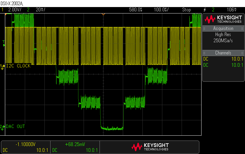
And by the way, the high noise frequency that I see on 1 step of the DAC is present also at 400KHz I2C bus speed. |
|
|
temtronic
Joined: 01 Jul 2010
Posts: 9115
Location: Greensville,Ontario
|
|
| Posted: Thu Mar 23, 2017 8:48 am |
|
|
re:...
the high noise frequency that I see on 1 step of the DAC is present also at 400KHz I2C bus speed.
OK , you need to find out WHERE that's coming from !!
Check the PIC power supply pins,in fact every pin on the PIC as well as the DAC.
What's the 'noise' look like? What frequency? Steady or pulsed? Amplitude? Wave shape?
Forget about a 'filter' until the noise is found and eliminated. |
|
|
viki2000
Joined: 08 May 2013
Posts: 233
|
|
| Posted: Thu Mar 23, 2017 9:09 am |
|
|
The tests done above were with 1.6MHz I2C bus speed and the lookup table had 170 entries for 0°-90° of the wave generating around 93Hz rectified sinewave.
Just to make everyone happy I came down to 400 KHz using next code:
| Code: | #include <PIC18F45K20.h>
#use delay(internal=64MHz, clock_out)
#use I2C(MASTER, scl=PIN_C3, sda=PIN_C4, FORCE_HW, FAST=400000)
CONST unsigned long SINE_WAVE[45] = {0, 29, 57, 86, 114, 142, 170, 198, 226, 253, 280, 307, 333, 359, 384, 409, 434, 458, 481, 504, 526, 548, 569, 589, 609, 627, 645, 663, 679, 695, 709, 723, 736, 748, 759, 770, 779, 787, 795, 801, 807, 811, 815, 817, 819};
void dac_i2c(unsigned int16 sample){
i2c_start(); // Start
i2c_write(0b11001000); // Device address
i2c_write(0b1000000); // Internal Device address
i2c_write((sample & 0xFF0) >> 4); // Upper data bits
i2c_write((sample & 0xF) << 4); // Lower data bits
i2c_stop(); // Stop
}
void main() {
setup_adc(ADC_OFF);
unsigned long int i=0;
disable_interrupts(GLOBAL);
while(TRUE){
while (i< 44){
i++;
delay_cycles (70);
dac_i2c(SINE_WAVE[i]);
}
output_toggle(PIN_D7);
while (i>0){
i--;
delay_cycles (70);
dac_i2c(SINE_WAVE[i]);
}
}
} |
The Sallen-Key filter 2nd order with R1,2=2K and C1,2=10nF and only 45 entries in lookup table for 0°-90° made an acceptable job with next waveforms:
https://goo.gl/Jqk4jS
I will stop here with the MCP4725 I2C DAC tests and I will focus, when the time permits, on MCP4921 SPI DAC. |
|
|
temtronic
Joined: 01 Jul 2010
Posts: 9115
Location: Greensville,Ontario
|
|
| Posted: Thu Mar 23, 2017 9:18 am |
|
|
| still a LOT of nise on the rw DAC output... interesting that there are 4 'bursts' per DAC bit, makes me curious as to where that comes from as 'zero' doesn't have it nearly as bad.... |
|
|
Ttelmah
Joined: 11 Mar 2010
Posts: 19229
|
|
| Posted: Thu Mar 23, 2017 10:32 am |
|
|
If you look at his original waveforms, they had four three spikes per DAC update. Four segments. Spikes were at exactly the same points in the waveforms as the gaps between the bursts are now. The I2C transaction, has 'start', two data bytes, then 'stop'. Four parts to each transaction. This is why I mentioned digital to analog crosstalk. It's odd that there are clocks in the start and stop 'parts'.
I wonder how the charge pump for the EEPROM inside the DAC is clocked?. |
|
|
viki2000
Joined: 08 May 2013
Posts: 233
|
|
| Posted: Fri Mar 24, 2017 1:30 am |
|
|
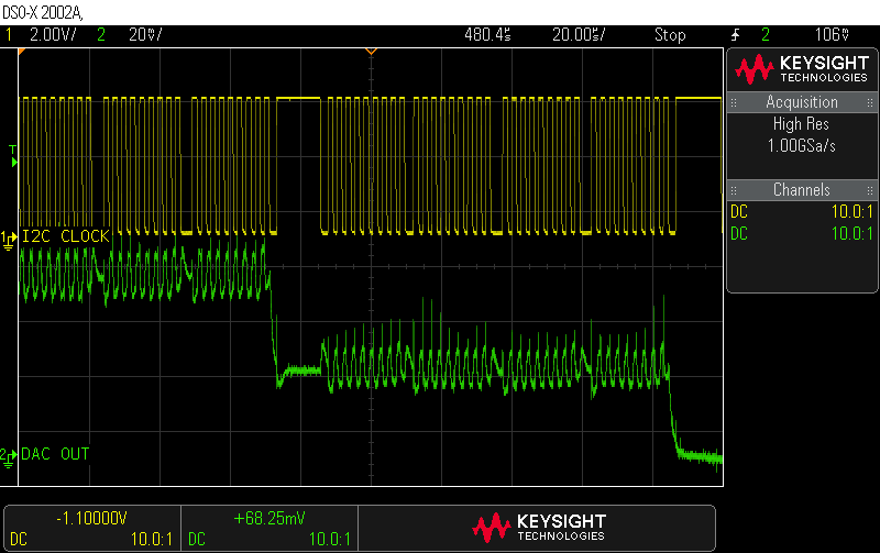
Ttelmah has an eagle eye:
 |
|
|
Ttelmah
Joined: 11 Mar 2010
Posts: 19229
|
|
| Posted: Fri Mar 24, 2017 2:02 am |
|
|
OK. Device address, command, two data bytes.
Direct digital crosstalk from the I2C.
This is 99% down to board layout, smoothing, and isolation.
Section 8.4 in the data sheet
| Quote: |
8.4 Layout Considerations
Inductively-coupled AC transients and digital switching
noise from other devices can affect on DAC
performance and DAC output signal integrity. Careful
board layout will minimize these effects. Bench testing
has shown that a multi-layer board utilizing a lowinductance
ground plane, isolated inputs, isolated
outputs and proper decoupling are critical to achieving
the performance that the MCP4725 is capable of
providing. Particularly harsh environments may require
shielding of critical signals. Separate digital and analog
ground planes are recommended. In this case, the VSS
pin and the ground pins of the VDD capacitors of the
MCP4725 should be terminated to the analog ground
plane.
|
Fiddling around filtering is not where to start. You need to remove this at source.
However if you do filter, you now know the fundamental frequency to remove. |
|
|
viki2000
Joined: 08 May 2013
Posts: 233
|
|
| Posted: Fri Mar 24, 2017 5:25 am |
|
|
My initial tests were done with PIC16F1825 on a breadboard.
My second tests were done with PIC18F45K20 on the Microchip Demo Board.
I did not design a special PCB in a CAD program for this small SOT-23-6 package and entire circuit, but I came back to 400KHz I2C bus speed and I have made a small test PCB for bench test purpose with PIC16F1825 that you may see in the link below.
I have changed from hardware I2C to software I2C only to have short and parallel connection between PIC and MCP4725. The pull-up resistors are 2.2K.
It seems a fair enough distance between I2C clock line SCL and the output of the DAC, but the noise is still there.
Would you have done a better PCB for first test purpose on the bench?
Please suggest what I should change on PCB in order to get rid of the SCL cross-talk noise on output of the DAC. Keep in mind that I can use only these PCBs for test, I have different types, but I will not make a special one with CAD software.
If this would have been for a design project, I would have changed/chosen since long time another DAC I2C from another company. I will stop using MCP4725 and make further tests.
It seems to me that MCP4725 is a little bugger and the noise comes from its womb.
https://goo.gl/yWIVQ9 |
|
|
newguy
Joined: 24 Jun 2004
Posts: 1902
|
|
| Posted: Fri Mar 24, 2017 6:12 am |
|
|
You need a 4 layer PCB, properly designed. You may be able to get by with a 2 layer PCB with ample ground pours and proper isolation between the I2C lines and the plane.
The MCP4725 is not sourcing noise "from its womb." Your noise problems are entirely of your own design as your boards are NOT adequate, and neither is your 5V rail. The TO-92 5V regulator you're using is probably rated for 100mA, and that, in my experience, is borderline for what you're attempting to power from it. |
|
|
viki2000
Joined: 08 May 2013
Posts: 233
|
|
|
temtronic
Joined: 01 Jul 2010
Posts: 9115
Location: Greensville,Ontario
|
|
| Posted: Fri Mar 24, 2017 7:18 am |
|
|
You've got to locate the source of the noise. Since it's very consistant, you should be able to track it down.
As for the PCB layout...2 sided will work. I designed 32 chnl/16 bit PMT acquistion boards for optical emission spectrometers back in late 70s. They could accurately read 1mv is a very,very EMI environment so I KNOW it can be done.
Your PCB needs PSU filtering, chokes, bypass caps, shielded box,a 'ring ' of ground bus.Every device needs bypass caps. I didn't use a 'flood' ground plane, instead used a 'grid' ground plane( X-Y .1 traces) as it reduced board warpage and was better in dealing with the RF In the spectrometer.
The 5V PSU is probably a switching style, so it needs more filtering and shielded wiring. The LM78L05 also needs additional help, see a datasheet.
RE PIC program. have you set any unused pin high or low? IE NOT floating.Also you need to disable the ADC section if not using it,same for the comparators.
You should also have a 'buffer' opamp from the DAC, properly loaded.
Is the scope properly grounded to the house wiring? A floating scope or bad 'earth' will induce noise aka EMI...
There's 100 things that can cause the problem and each and every one needs to be dealt with.
Doing analog is easy, with 8 bits it is a challenge, with 12 it can become a lifelong nightmare ! |
|
|
|
|
You cannot post new topics in this forum
You cannot reply to topics in this forum
You cannot edit your posts in this forum
You cannot delete your posts in this forum
You cannot vote in polls in this forum
|
Powered by phpBB © 2001, 2005 phpBB Group
|

