 |
 |
| View previous topic :: View next topic |
| Author |
Message |
temtronic
Joined: 01 Jul 2010
Posts: 9133
Location: Greensville,Ontario


|
|
 Posted: Tue Jan 31, 2017 6:33 am Posted: Tue Jan 31, 2017 6:33 am |
 |
|
Queitly following this thread and wondering why not just create a real sine wave and use a precision rectifer, with DC offset correction?
It might be easier and cheaper ? R&D time really does cost $$$
While there may be more parts,having the device 'up and running' quicker can easily offset the parts cost.
Just curious
Jay |
|
 |
viki2000
Joined: 08 May 2013
Posts: 233
|
|
| Posted: Tue Jan 31, 2017 6:59 am |
|
|
@Ttelmah
Why at 9v?
@temtronic
I am not paid for this. It is a job in-between tasks, when I have some time, it is more to increase my knowledge and hoping to achieve something in the end. |
|
|
temtronic
Joined: 01 Jul 2010
Posts: 9133
Location: Greensville,Ontario
|
|
| Posted: Tue Jan 31, 2017 8:10 am |
|
|
If you're not being paid for the project, you really need to consider the TIME you're spending on the project ! Life is waay too short.
The older you get, you realise that TIME is THE factor. The tape measure of life is only so long, so I now look at options,even though they may cost a bit more.
These days I can design on Monday,R&D on Tuesday, finalise on Wednesday, contact fab house in China on Thurday and by next MONDAY ,have complete ,working PCBs in my lab. Such is the power that is available today.
Jay |
|
|
viki2000
Joined: 08 May 2013
Posts: 233
|
|
| Posted: Tue Jan 31, 2017 8:36 am |
|
|
| You can, because you know enough, but does not apply to everyone, especially when someone is on the learning ramp in certain fields, maybe adjacent to the daily job, wanting to explore and then after a while comes the experience and knowledge and you may sit back and look over the past years, thinking at what you have done and at the things that you may accomplish now, but seen with different eyes, from different perspective, because you know more and then realize what you have lost, the time, which now you would like to have been used it different perhaps. It is the same game for all, no matter what we do. |
|
|
Ttelmah
Joined: 11 Mar 2010
Posts: 19255
|
|
| Posted: Tue Jan 31, 2017 8:45 am |
|
|
0v. Hit the key next to the one I was aiming for.....  |
|
|
asmboy
Joined: 20 Nov 2007
Posts: 2128
Location: albany ny

|
|
| Posted: Tue Jan 31, 2017 9:27 am |
|
|
| Quote: | | That box will test an existing product/device inserted in a slot/connector of the tester. The device to be tested, in the real application, is connected to mains after a rectifier bridge and detects when the rectified sine-wave touches 0V and measures also the voltage with an ADC 8bits. When will be tested with that portable tester, I should provide/simulate the full rectified sine-wave (as good as possible – defined below) which is seen by the device in the real application. That is all. |
the magic words - mains and test -
split my sides laughing  
any PIC generated signal can't compete for simplicity
or accurate test condition signal generation with the right hardware.
there is a circuit that will make the waveform you seek PERFECTLY
and with far less cost and complexity--
just do do this:
http://www.learnabout-electronics.org/PSU/images/bridge-rect-2.jpg |
|
|
viki2000
Joined: 08 May 2013
Posts: 233
|
|
| Posted: Wed Feb 01, 2017 1:12 am |
|
|
@asmboy
It is a portable "box" with only +5Vdc power supply.
I do not have any alternative power source, unless I generate it.
Of course it crossed to my mind to make a full sine-wave with a PIC and then to rectify it with a 4 diodes, a rectifier bridge, but that would imply to have +5V and +5V to center the wave and I wanted to avoid that. Besides, it might be a problem with drop voltage over the diodes and possible offset and I need my waveform to touch 0V.
I realize that we can debate here, because we can find small signal diodes with very low drop voltage or you may say that in the main application there is a rectifier bridge anyway and then we have the same problems, but is not quite like that. The real application has 230Vac input and after rectifier bridge there is a voltage divider 10M and 33K which provides around 1Vpp signal for an 8bit ADC. Then any offset or drop voltage over the diodes does not influence the 8bit ADC because is reduced with a factor of 3300.
I thought that it might be easier to generate directly a rectified sine wave. |
|
|
viki2000
Joined: 08 May 2013
Posts: 233
|
|
| Posted: Wed Feb 01, 2017 1:37 am |
|
|
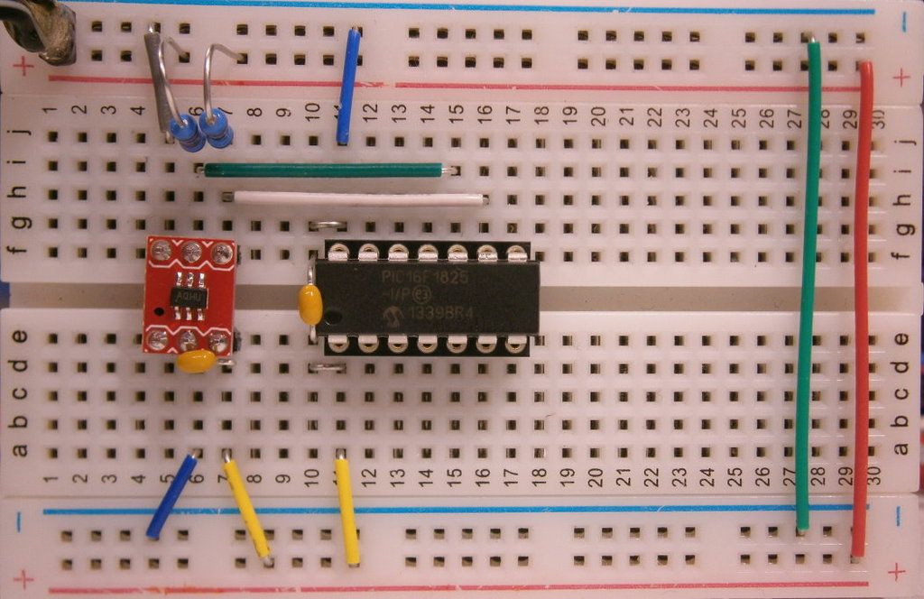
@Ttelmah
Regarding the layout, my tests with DAC were done on a simple breadboard as you may see below:
 |
|
|
Ttelmah
Joined: 11 Mar 2010
Posts: 19255
|
|
| Posted: Wed Feb 01, 2017 3:21 am |
|
|
| Honestly 'no wonder' you have noise problems..... |
|
|
Mike Walne
Joined: 19 Feb 2004
Posts: 1785
Location: Boston Spa UK
|
|
| Posted: Wed Feb 01, 2017 4:05 am |
|
|
You're asking for the impossible.
It's time for a rethink.
You've been told most of this already.
1) Your noise spikes are comparable to your step size near zero.
You must deal with the noise before even considering smaller steps.
Your white board layout is likely doomed to failure in this respect.
2) No amount of LP filtering will simultaneously smooth out the waveform and give a true zero.
Try it out on either pSpice or Excel to see what happens without your current noise issues, (no pun intended).
3) You can work out the harmonics exactly using Fourier analysis.
Mike
PS I do realise this is a blue sky project. |
|
|
viki2000
Joined: 08 May 2013
Posts: 233
|
|
| Posted: Wed Feb 01, 2017 5:39 am |
|
|
@Ttelmah
Do you mean due to breadboard used and the hundreds of KHz up to 1.9MHz frequencies involved?
Or do you refer to a better connection/layout on that breadboard?
If you refer to proper PCB with proper grounding instead of breadboard, then this is what I intend to do for next tests and that was the final project idea. I used the breadboard for a fast test to see if the code and the hardware work together, then I noticed the steps and noise.
@Mike Walne
Thank you for suggestions. Maybe I will do some software simulation analysis with a SPICE package later when I have time. |
|
|
temtronic
Joined: 01 Jul 2010
Posts: 9133
Location: Greensville,Ontario
|
|
| Posted: Wed Feb 01, 2017 6:36 am |
|
|
re: the breadboard.
Yes they are very, very bad for a lot of 'noise' reasons but...if you can get it to work on one of them, it'll work a LOT better with a PCB ! I've got some that are 25 years old and it's easy to grab and test for just a quik basic 'proof of concept'..then get a perfboard (solder pad per hole) and install sockets for PIC and other noise sensitive devices. I use stripped wirewrap wire to 'solder stitch' the connections.These 'stitches' are like PCB traces,just manually done. With a little practice, you can make a project faster than doing a PCB with resist pen, etchant and drilling.
Since this device will be plugged into Mains powered equipment, another option might be to program the PIC to send 100Hz to a center tapped audio transfomer. You might need a couple 2N3904s as buffers. The transformer secondary IS isolated and you only need to add a bridge to get the full wave, rectified 100Hz output signal you need. I built similar devices as 'wire tracers' and tazers before PICs had Flash memory in them.
Just trying to think of options for you....
Jay |
|
|
Ttelmah
Joined: 11 Mar 2010
Posts: 19255
|
|
| Posted: Wed Feb 01, 2017 7:58 am |
|
|
The other thing on the breadboard, is make a permanent addition of a couple of electrolytic capacitors across the supply busses.
Your supply is presumably coming from something like a bench supply, and with a length of wire between this and the board, there will be significant ripply on the rail.
It is possible to layout reasonable circuits with them, but a lot of care is needed. I'd probably lay the digital circuitry all out on one section of board, and then the analog on a separate section. Then a single ground connection from each 'back' to where the supply comes into the unit.
You need a couple of big terminals, for your supply. Take the grounds from each board section back to these, and your scope to the same point. Try to avoid 'daisy chain' supplies (yours is coming in at the top left I think and then 'daisying' on from top right to bottom right, and round. This is a recipe for differential voltages on this rail... |
|
|
Mike Walne
Joined: 19 Feb 2004
Posts: 1785
Location: Boston Spa UK
|
|
| Posted: Wed Feb 01, 2017 8:33 am |
|
|
Have you worked out yet where the roughly 20-25us spikes are coming from?
As a point of interest:-
I have seen a full wave rectified sine wave used in a real product.
A company I used to work for made power factor corrected battery chargers.
This was (and often still is) done by inserting a boost converter between the mains input rectifier and storage capacitor.
Before dedicated chips were availble they created a rectified sine wave as a reference signal.
The sine wave was created by an oscillator followed by an 8 bit divider and a DAC.
The oscillator was locked to the mains with a PLL.
The amplitude was variable by adjusting the DAC reference voltage.
One control loop forced the mains input current to follow the synthesised sine wave.
A second control loop adjusted the DAC reference as the power demand fluctuated.
All this was done at the behest of the client.
Nobody realised (or dared argue) that better PFC would be attained by making the mains input current follow the real distorted mains input voltage rather than forcing the input current to be sinusoidal!
Mike |
|
|
viki2000
Joined: 08 May 2013
Posts: 233
|
|
| Posted: Thu Feb 02, 2017 7:28 am |
|
|
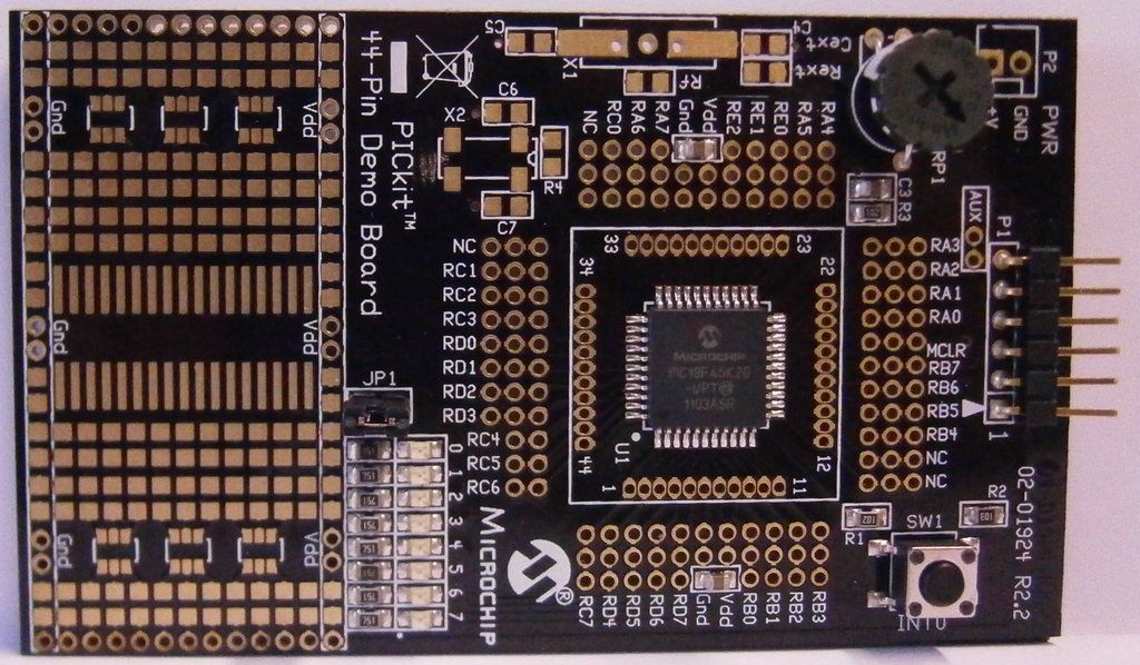
I noted down your suggestions.
I looked around and I found an unused new PIC Demo Board with PIC18F45K20, which can run at 64MHz with its inside PLL turned on.
I think this small board will eliminate any noise concern. I intend to use it, most probably, next week, if I have time. It seems the proper board for such kind of small test.
http://www.microchip.com/DevelopmentTools/ProductDetails.aspx?PartNO=dm164130-4
http://ww1.microchip.com/downloads/en/DeviceDoc/41296B.pdf
Now I see 2 options:
1) I have a nice wave with less noise and after filtering the result is acceptable, all these with only 100 points for 10ms (at 600 KHz set in CCS) or 170 points (at 1.9 MHz set in CCS) and I stop here.
2) I increase the I2C speed up to 3.4 MHz, supported by the MCP4725, and then I can enlarge the look-up table.
When I measured with the oscilloscope the I2C clock and I compared with the speed set in CCS at FAST=, then I noticed next differences due to subroutine execution delays related with the internal oscillation frequency of the PIC at 32 MHz:
- FAST=100000 (100KHz) is the same as I would not mention FAST at all and the I2C clock was 98.5KHz
- FAST=400000 (400KHz) gave I2C clock of 380KHz
- FAST=600000 (600KHz) gave I2C clock of 533KHz
- FAST=1900000 (1.9MHz) gave I2C clock of 1.3MHz
For the 2) option I have some questions:
- What is the maximum speed supported by PIC I2C bus in general or at least for some PICs as 18F45K20 or 16F1825 or any other? How do you find that and how do you set it?
I know, looking at the block diagram of the I2C inside the PIC that is a register that takes care of the baud generator as it is also explained in the next document at the pages 49-50:
http://ww1.microchip.com/downloads/en/DeviceDoc/i2c.pdf
Then in my case SSPADD must be 4 if I run the PIC at 64MHz, but how do we do it with CCS? Only writing FAST=34000000?
- Assuming the PIC is able to run the I2C at 3.4MHz, is the I2C subroutine from CCS able to keep up with that speed using the PIC at 64MHz? Or do I have to write my own I2C subroutine in a XC8 manner to set different the registers and I2C speed?
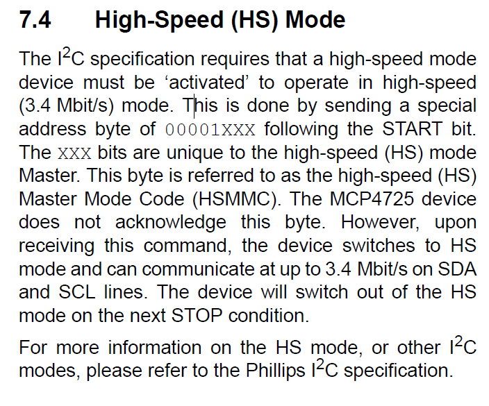
The last thing that twists my mind is the High Speed Master Mode Code. Without that code, the MCP4725 cannot communicate up to 3.4 Mbit/s, so it is important.
Where do I find that code, those 4 bits?
 |
|
|
|
|
You cannot post new topics in this forum
You cannot reply to topics in this forum
You cannot edit your posts in this forum
You cannot delete your posts in this forum
You cannot vote in polls in this forum
|
Powered by phpBB © 2001, 2005 phpBB Group
|

