 |
 |
| View previous topic :: View next topic |
| Author |
Message |
newguy
Joined: 24 Jun 2004
Posts: 1932


|
| Working Optrex F-51852 (NJU6676) init code & h/w connect |
 Posted: Tue Apr 03, 2007 3:31 pm Posted: Tue Apr 03, 2007 3:31 pm |
 |
|
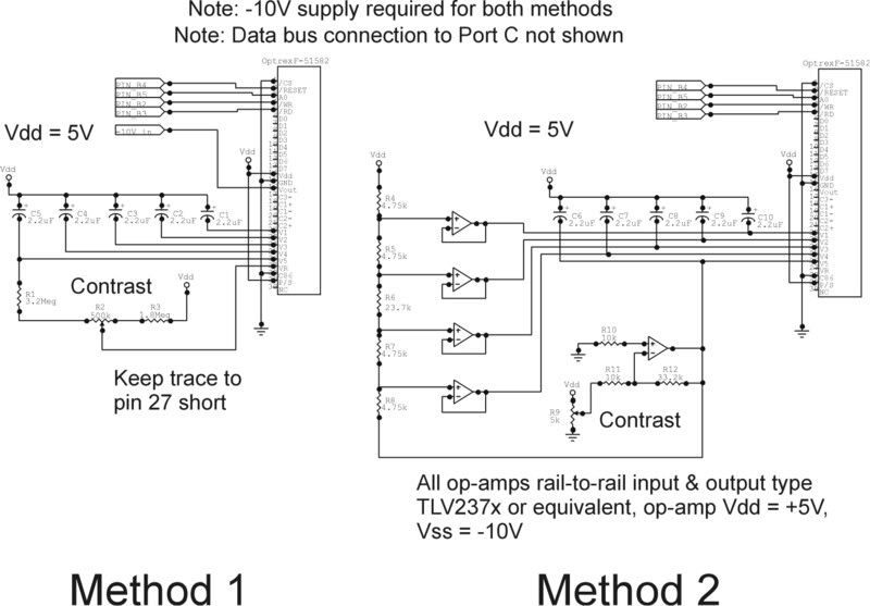
I had a devil of a time getting an Optrex F-51852 128x64 graphical display to initialize properly, so I'm posting the working code here in case anyone else runs into the same problems I did.
Optrex doesn't recommend using the internal charge pumps to create the LCD drive voltages for the NJU6676 controller. I am posting two different connections/methods of driving this display. The code is clearly commented as to which h/w layout each pertains to.
The 2.2 uF capacitors I used in the schematic are simply what I had on hand. Optrex recommends using these particular capacitors:
4.7uf, NACEW4R7M35V4X5.5TR13 MFG: NIC
1uf, UWX1H010MCR1GB MFG: NIC
For what it's worth, I've seen 'reference' designs that use 0.1 to 4.7 uF capacitors, so size doesn't seem to be an issue.
The connections are as follows: 
To initialize the LCD, simply call:
NOTE: Allow for a 100 millisecond delay after the PIC powers up before attempting the LCD init routine.
Here is the driver code, as tested using an 18F4680:
| Code: | #define ON 1
#define OFF 0
#define YES 1
#define NO 0
struct lcd_pin_def
{
int data : 8;
};
#define LCD_WR PIN_B2
#define LCD_RD PIN_B3
#define LCD_RESET PIN_B4
#define LCD_A0 PIN_B5
#define set_tris_lcd(x) set_tris_c(x);
struct lcd_pin_def GLCD;
#byte GLCD = 0xf82 // port c on the 18f4680
void glcd_writeByte(int1 DI, int data);
void glcd_init(void);
void glcd_init(void) {
output_low(LCD_RESET); // hard reset
delay_us(20);
output_high(LCD_RESET);
delay_ms(100);
// init code for h/w connection METHOD 1
glcd_writeByte(0, 0xE2);
glcd_writeByte(0, 0xb0);
glcd_writeByte(0, 0x10);
glcd_writeByte(0, 0x00);
glcd_writeByte(0, 0xa1);
glcd_writeByte(0, 0x81); // contrast set
glcd_writeByte(0, 0x3f); // contrast set
glcd_writeByte(0, 0xaf);
glcd_writeByte(0, 0x2b);
delay_ms(50);
glcd_writeByte(0, 0xe7);
// note that with this method, the contrast is s/w adjustable
// init code for h/w connection METHOD 2
/*glcd_writeByte(0, 0xE2);
glcd_writeByte(0, 0xa2);
glcd_writeByte(0, 0xa1);
glcd_writeByte(0, 0xc0);
glcd_writeByte(0, 0x40);
glcd_writeByte(0, 0x28);
glcd_writeByte(0, 0xa4);
glcd_writeByte(0, 0xa6);
glcd_writeByte(0, 0xe7);
glcd_writeByte(0, 0xaf);*/
}
void glcd_writeByte(int1 DI, int data) {
if (DI) {
output_high(LCD_A0);
}
else {
output_low(LCD_A0);
}
set_tris_lcd(0x00);
GLCD.data = data;
delay_us(2);
output_low(LCD_WR);
delay_us(2);
output_high(LCD_WR);
set_tris_lcd(0xff);
} |
|
|
 |
nickd
Joined: 30 Jun 2008
Posts: 2
Location: Adelaide, Australia


|
|
 Posted: Mon Jun 30, 2008 2:01 am Posted: Mon Jun 30, 2008 2:01 am |
 |
|
Hi there,
This post is fairly old I know, however I'm currently having problems getting one of these to work.
I've tried your initialisation sequence and it doesn't work for me. What I had already was quite similar... although the order was different. I'm using a 3.3V supply and Method 1.
You said you had trouble getting it to work... what was the actual trick, ie what was it that you changed for it to work? The order of initialisation? The settings themselves?
I notice that in the Method 1 code you initialise the Column and Row addresses before you initialise any of the control registers.. yet you don't do this in the Method 2 code... is this intentional?
The various datasheets I've looked at suggest that power sequencing is important.. your schematic doesn't show any control over the -10V supply.. did you have any problems with this?
Cheers,
Nick |
|
 |
newguy
Joined: 24 Jun 2004
Posts: 1932


|
|
 Posted: Mon Jun 30, 2008 8:30 am Posted: Mon Jun 30, 2008 8:30 am |
 |
|
My system uses a 5V supply and method 1. The trouble I was having was that the NJU6676 was supposed to be a direct pin-for-pin replacement for the Epson SED controller on earlier versions of this display (Optrex F-51320, and another F-5something display). It isn't. Not even close. At least the Epson controller's internal charge pump actually works. The NJU6676's doesn't.
The problem I had was a) connection and external Vref drive and b) s/w init of the display. Once I stumbled upon an init sequence that worked for me, I locked it in. The original post is the result. The non-initialization of the column & row addresses in method 2 was based on some sample code (in assembly) that I got from an Optrex support engineer. Method 1's code was based on that sample code too.
Power sequencing: I remember worrying about this, but my end circuit worked without actually having to do it. My power circuitry is very straightforward. Just direct connections to 5V Vcc and I generate -10V with a pair of TI TPS6040 charge pumps. The circuit I use is directly from the datasheet, http://focus.ti.com/lit/ds/symlink/tps60400.pdf. It's Figure 28, the doubling inverter, found on page 16. Perhaps the inverter takes some time after the 5V rail has come up to establish itself. That said, I didn't have any problems getting the display to work when I was just using a lab supply to generate -10V and I didn't need to apply/bring up the supplies in any particular order.
At 3.3V perhaps power sequencing is more important. Try it and see if it helps. If not, get in contact with Optrex for help. Just remember that the US has their 4th of July holiday coming up quickly. |
|
 |
nickd
Joined: 30 Jun 2008
Posts: 2
Location: Adelaide, Australia


|
|
 Posted: Mon Jun 30, 2008 5:58 pm Posted: Mon Jun 30, 2008 5:58 pm |
 |
|
Hi there,
Thanks for the prompt reply 
I discovered last night that the bulk of my problems were due to (my own!) dodgy soldering on the FPC connector.. so I have progress and an image on the screen... albeit almost invisible, so I have some work to do on the contrast settings.
Thanks for the tip on the charge pumps.. will have a look at those.
Cheers,
Nick |
|
 |
|
|
You cannot post new topics in this forum
You cannot reply to topics in this forum
You cannot edit your posts in this forum
You cannot delete your posts in this forum
You cannot vote in polls in this forum
|
Powered by phpBB © 2001, 2005 phpBB Group
|


